RV740 chipset specifications
Okay then, you fine men and women would of course like to learn everything about this little silicon called RV740. So, we'll try to get you as much information as we can gather. But obviously we have only very limited information at hand.
A good way to explain a product is to always explain what it is not.
RV740 is not a high-end graphics card. In fact if the board partner that submitted this card is correct, it's pricing would be below 99 USD. That would make it fare into the budget segment. But it's not a budget product either.
The chip will be the successor to the RV730 (Radeon HD 4650/4670), although that product will still remain in the market for a while, we think, AMD can redefine the budget to middle class product line-up. See, performance of the strongest RV740 based product will move upwards in-between HD 4830 and HD 4850 performance.
It is a very spiffy card when it comes to performance (for the money of course). Here's what we know. RV740 has 640 shaders (stream processors). The core frequency for the early engineering sample card we tested is 650 MHz.
RV740 is based off a 40nm production node and is equipped with 128-bit memory. Now before your go "aaahw, we lost half the framebuffer bandwidth due to 128-bit memory", here's the thing. The RV740 is equipped with GDDR5 memory. This GDDR5 memory is running at 800 MHz, that would boil down to 3200 MHz, 3.2 Gbps effective... that's just over 50 GB/sec of bandwidth depending on the final memory configuration.
Now if you cut down the memory bus in half to 128-bit you lose half the bandwidth, ATI compensates for that by doubling it up again with GDDR5 memory. It's a bit of a tradeoff here and there. See, 128-bit memory is fairly cheap to use and does return a heap of framebuffer bandwidth thanks to the higher frequency memory. Also I can imagine a simpler design in the PCB such as using less wires and thus a cheaper design. On the flip side, slower memory latency timings. But granted, this choice makes a lot of sense, as the results will show.
Now I've fired off some math at the most generic denominators and when we place things in a chart, you'll gain some perspective of product differences.
|
ATI Radeon |
ATI Radeon |
RV740 HD 4750 |
ATI Radeon HD 4670 |
ATI Radeon HD 3870 | |
| # of transistors |
956 million |
956 million |
826 million |
514 million | 666 million |
|
Stream Processing Units |
800 |
640 |
640 | 320 | 320 |
|
Clock speed |
625 MHz |
575 MHz |
650-700 | 750 MHz | 775+ MHz |
|
Memory Clock |
2000 MHz GDDR3 (effective) |
1800 MHz GDDR3 (effective) |
3200 MHz GDDR5 (effective) |
2.0 GHz GDDR3 (effective) | 2.25 GHz GDDR3 (effective) |
|
Math processing rate (Multiply Add) |
1000 GigaFLOPS |
740 GigaFLOPS |
960* GigaFLOPS |
480 GigaFLOPS | 497+ GigaFLOPS |
|
Texture Units |
40 |
32 |
32 | 32 | 16 |
|
Render back-ends |
16 |
16 |
16 | 8 | 8 |
|
Memory |
512MB GDDR3 |
512MB GDDR3 |
512MB GDDR5 | 512MB GDDR3 | 512MB GDDR3/4 |
|
Memory interface |
256-bit |
256-bit |
128-bit | 128-bit | 256-bit |
|
Fabrication process |
55nm |
55nm |
40nm | 55nm | 55nm |
|
Power Consumption (peak) |
~110W |
~110W |
tba | ~59W | ~105W |
* estimate based on early engineering sample card
The RV740 houses 640 stream processors, 32 texture memory units (TMUs) and 16 render output units (abbreviated as ROPs). As stated, It features a 128-bit wide bus using GDDR5 memory, bumping up bandwidth that rivals equally clocked GDDR3 with double the bus width. Very interesting.
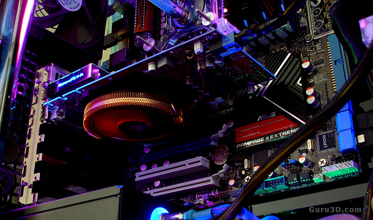
Now with this engineering sample in house we feel it's not fair to include numbers on heat, noise and power consumption. The specs are not yet 100% finalized, neither was power management and as such it would be unfair to include. So we'll hop straight onwards to a photo-shoot and then will fire up a couple of benchmarks to see where the product is going to position itself.